空军工程大学 航空机务士官学校, 河南 信阳 464000
工艺差异引起的Fin结构变化会造成纳米FinFET器件呈现不同的电学特性,使器件的单粒子瞬态效应(SET)复杂化。基于电学特性校准的14 nm SOI 标准型FinFET器件,构建了弹头型、三角型、阶梯型、半圆型及底部椭圆型等5种结构,分析了SET的表征量与Fin结构参数间的相关性,并利用灰色理论,研究了它们之间的内在关联性。结果表明,器件的收集电荷量、沉积电荷量与Fin的截面积显著相关;SET电流峰值、电子-空穴对产生率峰值及双极放大系数同时依赖于Fin的截面积和等效沟道宽度,且对等效沟道宽度的依赖性更强。
单粒子瞬态 Fin结构 相关性 工艺差异 FinFET FinFET single event transient fin structure correlation process variation
Author Affiliations
Abstract
1 Beijing National Research Center for Information Science and Technology (BNRist) and Department of Electronic Engineering, Tsinghua University, Beijing 100084, China
2 State Key Laboratory of Information Phonetics and Optical Communications, Beijing University of Post and Telecommunications, Beijing 100876, China
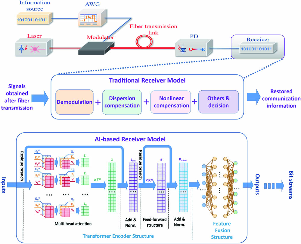
In this paper, an artificial-intelligence-based fiber communication receiver model is put forward. With the multi-head attention mechanism it contains, this model can extract crucial patterns and map the transmitted signals into the bit stream. Once appropriately trained, it can obtain the ability to restore the information from the signals whose transmission distances range from 0 to 100 km, signal-to-noise ratios range from 0 to 20 dB, modulation formats range from OOK to PAM4, and symbol rates range from 10 to 40 GBaud. The validity of the model is numerically demonstrated via MATLAB and Pytorch scenarios and compared with traditional communication receivers.
fiber receiver model neural networks multi-head attention mechanism Chinese Optics Letters
2023, 21(3): 030602
Author Affiliations
Abstract
1 Beijing National Research Center for Information Science and Technology (BNRist), Department of Electronic Engineering, Tsinghua University, Beijing 100084, China
2 State Key Laboratory of Advanced Optical Communications System and Networks, Department of Electronics, School of Electronics Engineering and Computer Science, Peking University, Beijing 100871, China
3 State Key Laboratory of Advanced Optical Communication Systems and Networks, Intelligent Microwave Lightwave Integration Innovation Center (imLic), Department of Electronic Engineering, Shanghai Jiao Tong University, Shanghai 200240, China
Microwave photonic receivers are a promising candidate in breaking the bandwidth limitation of traditional radio-frequency (RF) receivers. To further balance the performance superiority with the requirements regarding size, weight, and power consumption (SWaP), the implementation of integrated microwave photonic microsystems has been considered an upgrade path. However, up to now, to the best of our knowledge, chip-scale fully integrated microwave photonic receivers have not been reported due to the limitation of material platforms. In this paper, we report a fully integrated hybrid microwave photonic receiver (FIH-MWPR) obtained by comprising the indium phosphide (InP) laser chip and the monolithic silicon-on-insulator (SOI) photonic circuit into the same substrate based on the low-coupling-loss micro-optics method. Benefiting from the integration of all optoelectronic components, the packaged FIH-MWPR exhibits a compact volume of and low power consumption of 1.2 W. The FIH-MWPR supports a wide operation bandwidth from 2 to 18 GHz. Furthermore, its RF-link performance to down-convert the RF signals to the intermediate frequency is experimentally characterized by measuring the link gain, the noise figure, and the spurious-free dynamic range metrics across the whole operation frequency band. Moreover, we have utilized it as a de-chirp receiver to process the broadband linear frequency-modulated (LFM) radar echo signals at different frequency bands (S-, C-, X-, and Ku-bands) and successfully demonstrated its high-resolution-ranging capability. To the best of our knowledge, this is the first realization of a chip-scale broadband fully integrated microwave photonic receiver, which is expected to be an important step in demonstrating the feasibility of all-integrated microwave photonic microsystems oriented to miniaturized application scenarios.
Photonics Research
2022, 10(6): 06001472
清华大学 电子工程系/北京信息科学与技术国家研究中心, 北京 100084
微波光子射频前端具有频率覆盖范围大、工作波段和瞬时带宽可灵活重构、抗电磁干扰等优势, 在泛在无线通信、软件无线电、雷达和电子战系统中有着广阔的应用前景。为进一步减小系统的尺寸和功耗以满足实际应用的需求, 构建基于光子集成芯片技术的微波光子射频前端微系统势在必行。文章分析了集成微波光子射频前端微系统目前在器件层面和系统集成层面面临的挑战, 并从高精细、可重构的光滤波器设计、混合集成系统架构设计和系统频率漂移抑制方案三个方面重点介绍了作者所在课题组开展的关于混合集成可重构微波光子射频前端的研究现状。
微波光子 集成光子 射频前端 混合集成 microwave photonics integrated photonics RF frontend hybrid integration
Author Affiliations
Abstract
1 Department of Electronic Engineering, Tsinghua University, Beijing 100084, China
2 Beijing National Research Center for Information Science and Technology (BNRist), Beijing 100084, China
A hybrid integrated low-noise linear chirp frequency-modulated continuous-wave (FMCW) laser source with a wide frequency bandwidth is demonstrated. By employing two-dimensional thermal tuning, the laser source shows frequency modulation bandwidth of 10.3 GHz at 100 Hz chirped frequency and 5.6 GHz at 1 kHz chirped frequency. The intrinsic linewidth of 49.9 Hz with 42 GHz continuous frequency tuning bandwidth is measured under static operation. Furthermore, by pre-distortion linearization of the laser source, it can distinguish 3 m length difference at 45 km distance in the fiber length measurement experiment, demonstrating its application potential in ultra-long fiber sensing and FMCW light detection and ranging.
Photonics Research
2021, 9(10): 10001948

Author Affiliations
Abstract
1 Beijing National Research Center for Information Science and Technology (BNRist), Beijing 100084, China
2 Department of Electronic Engineering, Tsinghua University, Beijing 100084, China
For moving objects, 3D mapping and tracking has found important applications in the 3D reconstruction for vision odometry or simultaneous localization and mapping. This paper presents a novel camera architecture to locate the fast-moving objects in four-dimensional (4D) space (, , , ) through a single-shot image. Our 3D tracking system records two orthogonal fields-of-view (FoVs) with different polarization states on one polarization sensor. An optical spatial modulator is applied to build up temporal Fourier-phase coding channels, and the integration is performed in the corresponding CMOS pixels during the exposure time. With the 8 bit grayscale modulation, each coding channel can achieve 256 times temporal resolution improvement. A fast single-shot 3D tracking system with 0.78 ms temporal resolution in 200 ms exposure is experimentally demonstrated. Furthermore, it provides a new image format, Fourier-phase map, which has a compact data volume. The latent spatio-temporal information in one 2D image can be efficiently reconstructed at relatively low computation cost through the straightforward phase matching algorithm. Cooperated with scene-driven exposure as well as reasonable Fourier-phase prediction, one could acquire 4D data (, , , ) of the moving objects, segment 3D motion based on temporal cues, and track targets in a complicated environment.
Photonics Research
2021, 9(10): 10001924
红外与激光工程
2021, 50(7): 20211045
1 清华大学电子工程系, 北京 100084
2 北京信息科学与技术国家研究中心, 北京 100084
空间叠层衍射成像是一种基于相干光的无透镜成像方式,因此可以避免透镜系统孔径有限带来的衍射极限问题。目前,空间叠层衍射成像方案多采用机械结构对光探针进行平移,这种方式会使光探针的位置产生偏移误差,导致成像质量的下降。为解决这一问题,利用硅基光子集成技术设计并制作了基于滤波器件的光束空间分配芯片,该芯片上共有16个发射天线,相当于16个光探针,光探针阵列以一定的交叠率照射物体,其衍射图样强度被红外相机的不同感光区域记录。该芯片可以替代传统的机械式光探针来实现空间叠层衍射成像。百纳米级的加工工艺降低了光探针位置的偏移误差,提高了成像的质量和系统的稳定性。同时,由于集成芯片的尺寸仅有毫米级别,故成像系统的尺寸也可相应地减小。
中国激光
2021, 48(15): 1517004

Author Affiliations
Abstract
1 Department of Electronic Engineering, Tsinghua University, Beijing 100084, China
2 Beijing National Research Center for Information Science and Technology (BNRist), Beijing 100084, China
The novel camera architecture facilitates the development of machine vision. Instead of capturing frame sequences in the temporal domain as traditional video cameras, FourierCam directly measures the pixel-wise temporal spectrum of the video in a single shot through optical coding. Compared to the classic video cameras and time-frequency transformation pipeline, this programmable frequency-domain sampling strategy has an attractive combination of characteristics for low detection bandwidth, low computational burden, and low data volume. Based on the various temporal filter kernel designed by FourierCam, we demonstrated a series of exciting machine vision functions, such as video compression, background subtraction, object extraction, and trajectory tracking.
Photonics Research
2021, 9(5): 05000701


